In PCB proofing, alumina ceramic substrate has been widely used in many industries. However, in specific applications, the thickness and specification of each alumina ceramic substrate are different. What is the reason for this?
1. The thickness of alumina ceramic substrate is determined according to the function of the product
The thicker the thickness of alumina ceramic substrate, the better the strength and the stronger the pressure resistance, but the thermal conductivity is worse than that of thin alumina ceramic substrate; On the contrary, the thinner the alumina ceramic substrate, the strength and pressure resistance are not as strong as thick, but the thermal conductivity is stronger than thick. The thickness of alumina ceramic substrate is generally 0.254mm, 0.385mm and 1.0mm/2.0mm/3.0mm/4.0.mm.
2. The size of alumina ceramic substrate is also different
Generally, alumina ceramic substrate is much smaller than ordinary PCB board as a whole, and its size is generally no more than 120mmx120mm. Those exceeding this size generally need to be customized. In addition, the size of alumina ceramic substrate is not the bigger the better, mainly because its substrate is made of ceramics. In the PCB proofing process, it is easy to cause the plate to break, resulting in a lot of waste.
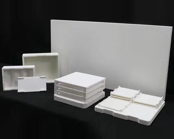
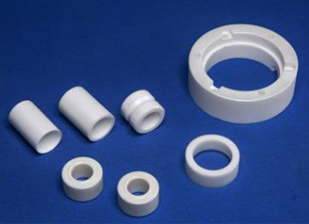
3. The shape of alumina ceramic substrate is different
Most of the alumina ceramic substrates are single and double-sided plates with rectangular, square and circular shapes. In PCB proofing, according to the process requirements, some also need to make grooves on the ceramic substrate, dam enclosing process, etc.


 QQ
QQ