


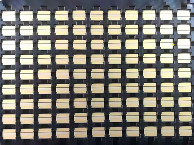
Shandong houfa New Material Co., Ltd
Mr Lu:15064141118
Ms zhang:18953321267
E-mail:zhangniandong@sdhofa.com
Add:Zhangqiu SME Transformation and Development Demonstration Park, Zhangqiu District, Jinan City, Shandong Province
|
project |
unit |
Al2O3 |
Al2O3 |
AlN |
Si3N4 |
|
content |
% |
96 |
99.6 |
/ |
/ |
|
density |
g/cm3 |
3.7 |
3.9 |
3.3 |
3.3 |
|
thermal conductivity |
25℃(W/m.K) |
>24 |
≥30 |
>170 |
>83 |
|
coefficient of thermal expansion |
(25-300℃)x10-6/℃ |
7.0 |
7.2 |
4.6 |
2.9 |
|
flexural strength |
MPa |
>350 |
>420 |
>310 |
>830 |
|
modulus of elasticity |
GPa |
>320 |
>380 |
>320 |
>320 |
|
dielectric constant |
1MHz |
9.4 |
9.9 |
8.5 |
9.0 |
|
Tangent of dielectric loss angle |
1MHz |
0.0004 |
0.0001 |
0.0003 |
0.002 |
|
electric strength |
KV/mm |
>15 |
>15 |
>14 |
>15 |
|
volume resistivity |
25℃(Ω·cm ) |
>1014 |
>1014 |
>1014 |
>1014 |
|
substrate thickness |
0.15mm |
0.2mm |
0.25mm |
0.3mm |
0.381mm |
0.5mm |
0.635mm |
|
|
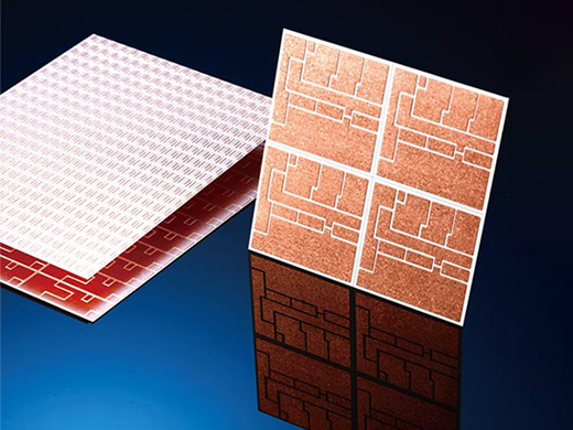
metal layer condition |
Ti layer: 80-150nm; Cu transition layer: 600nm; Cu electroplating layer: 3-100μm; |
|||||||
|
project |
unit |
Al2O3(96%) |
Al2O3(99.6%) |
AlN |
Si3N4 |
|
Maximum size |
mm |
101.6*101.6 |
101.6*101.6 |
101.6*101.6 |
101.6*101.6 |
|
Boundary dimension tolerance |
mm |
±0.1 |
±0.1 |
±0.1 |
±0.1 |
|
Product thickness tolerance |
/ |
±7% |
±7% |
±7% |
±7% |
|
line width, line spacing |
mm |
≥0.05 |
≥0.05 |
≥0.05 |
≥0.05 |
|
warp |
/ |
≤4‰ |
≤4‰ |
≤4‰ |
≤4‰ |
|
solderability |
/ |
>95 |
>95 |
>95 |
>95 |
|
Ra of copper surface |
μm |
≤1 |
≤1 |
≤1 |
≤1 |
|
Application temperature range |
℃ |
(-55,600) |
(-55,600) |
(-55,600) |
(-55,600) |
|
surface treatment |
Anti-oxidation treatment Thickness of surface nickel plating: 1-7μm Thickness of gold plating on the surface: 0.1-3μm Surface nickel-gold plating |
||||
 QQ
QQ